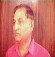
Dr. A. K. Saxena
 Dr. A. K. Saxena was born
at Rampur (U.P.) in India on july 1st, 1950. Dr. Saxena
obtained M.Sc. from Agra
University in 1969 from undivided Agra University, M.Sc.(Tech.). from
Department of Electronics and Electrical Engg.,B.I.T.S.
in 1971, M.Engg. and Ph.D. from Department of Electronics and
Electrical Engg.,UMIST/Sheffield
University (UK) in 1975 and 1978, respectively as one of the two Government
of India National Scholars. Served CEERI, a sister laboratory of CSIR
from 1972-74 working on semiconductor device technology and then served
University of Roorkee (Now IIT-Roorkee)
as Reader from 1978-88.
Since 1988, he is a Professor in Solid State Electronics. He has also spent a
year with Standard Telecommunication Laboratory (London) working on III-V
compound characterization under pressure.
Dr.
Saxena is a member of Overseas Advisory Board
of IEICE Transactions of Electronics of Japan since 1992. He is also a
Fellow, Honorary Editor and Member Editorial Board of IETE, one
of the three Fellows in semiconductors from India of Institute of
Physics (London) and Chartered Physicist of Institute of Physics
(London).
The discovery of a level in GaAlAs
is christened as 'Saxena's Deep Donor' by
Philips Research Laboratory, Netherlands.
He is also a winner of INSA
Young Scientist, Roorkee University Khosla Award Gold Medal, Kothari Scientific Research Institute Award and S.
K. Mitra Memorial Awards (twice) of IETE. He
is also a member of Research Board of Advisors of ABI (USA).He
has also been honored with the title of 'Man of the Year' by ABI (USA) and IBC
(UK). He is also an expert member on many National Committees and referee
for international journals/conferences.
Dr.
Saxena has visited several countries viz., UK, USA,
Japan, Australia, Romania and Thailand. He has also been a Royal Society
(London) - INSA visiting fellow and SERC (UK) senior visiting fellow at
University of Surrey (UK).He was also awarded visiting fellowship by University
of Michigan (USA). He has published about 150 research papers in international
journals and conference proceedings with very high citation index. He has
also been Investigator-in-charge of several projects from DST, INSA, CSIR, UGC,
etc. He also received financial assistance from NTT (Japan),IMT
(Romania),DST, INSA, AICTE, DOE, UP Govt., Ministry of Education & Social
Welfare and UOR/IIT for attending conferences abroad. Some of his research work
has been included in books published from USA and Germany. His biography has
been published in a large numbers of publications from U.K., U.S.A., Malaysia
and India.
Dr.
Saxena has supervised many Ph.D./M.E./M.Tech./M.Phil. thesis in the area of metal-semiconductor ohmic and non-ohmic contacts,
band structure and deep energy levels of GaAs, GaAlAs, GaP, InP,
etc and quantum wells under pressure. He has also written AICTE sponsored
nine volumes on the related subjects for working professionals.
Abstract: SEMICONDUCTORS AND DEVICES
UNDER STRESS